How to Use Die Bonding Tool for Effective Applications?
Using a Die Bonding Tool effectively is crucial for precision manufacturing. This tool plays a significant role in the assembly of microelectronic components. Proper application can enhance the performance of various products. Yet, many users struggle to maximize its potential.
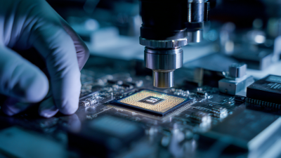
The Die Bonding Tool allows for accurate placement of semiconductor dies onto substrates. Understanding its features is essential. Users often rush through setups and miss critical adjustments. This can lead to alignment errors and reduced reliability. Recognizing the importance of these details can make a difference in production quality.
With hands-on practice and attention to detail, anyone can improve their skills. The tool requires familiarity and patience. Mistakes are common, but they offer valuable lessons. Reflecting on these challenges can lead to better outcomes in the long run. A well-used Die Bonding Tool can elevate production standards significantly.
Understanding Die Bonding Tools and Their Significance
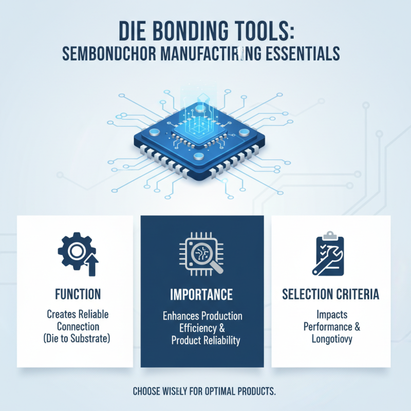
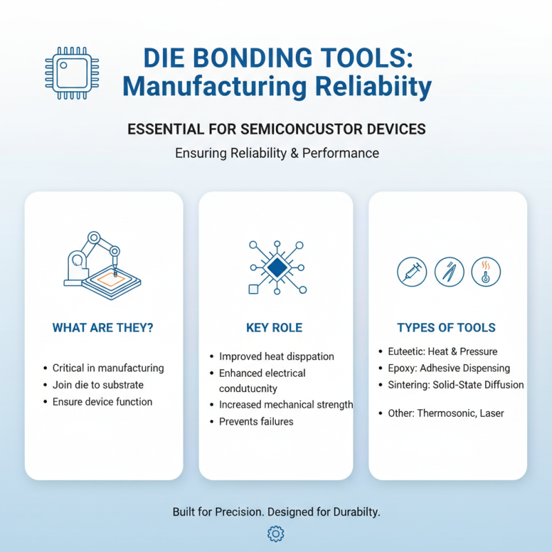
Die bonding tools are essential in semiconductor manufacturing. They create a reliable connection between the die and the substrate. Understanding these tools enhances production efficiency. Choosing the right type of die bonding tool is critical. It impacts the overall performance and reliability of the products.
Tips: Ensure you have the correct temperature settings. An inadequate temperature can compromise the bonding process. Maintain cleanliness of tools and work areas. Contaminants can lead to defects and costly rework.
Check the alignment carefully during bonding. Misalignment may cause failures down the line. The right pressure is crucial too. Too much pressure can damage delicate components. Inspect the results regularly and reflect on potential improvements. Status checks can save future headaches.
Types of Die Bonding Tools and Their Unique Features
Die bonding tools are essential in many manufacturing processes. They play a critical role in ensuring the reliability of semiconductor devices. There are various types of die bonding tools, each designed with unique features to meet specific needs.
Wire bonders are one common type. They provide precision for attaching wires from the die to the package. Often considered user-friendly, they can sometimes produce inconsistent results if not calibrated properly. Flip-chip bonders are another option. These tools offer the advantage of direct attachment without wires, yet their complexity can lead to longer learning curves.
Then, there are adhesive-based methods. These can be simpler but may require thorough surface preparation. Inadequate cleaning can lead to poor adhesion. It's crucial to understand the nuances of each type. Choosing the wrong tool can result in defects or reduced performance. Sometimes, even experienced users may find themselves frustrated with unexpected outcomes.
Preparation Steps for Effective Die Bonding Applications
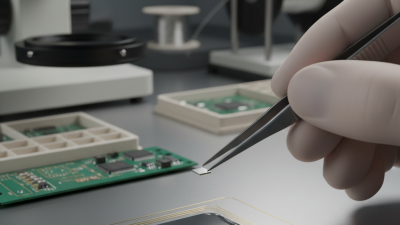
Die bonding is a critical process in semiconductor manufacturing. Preparation is key to achieving effective die bonding applications. An accurate setup can minimize errors and improve yield.
Start by ensuring the work area is clean and organized. Contaminants can lead to defects. A tidy environment helps maintain focus. Next, check that all tools, such as the die bonding tool itself, are calibrated and functioning correctly. According to industry reports, nearly 20% of defects arise from improper tool settings. This statistic highlights why calibration is crucial.
**Tip:** Regularly inspect your tools for wear and tear. This maintenance can prevent unexpected failures.
Before commencing, verify the materials used for bonding. Each type of die requires specific adhesives or pastes. Using the wrong material can result in weak bonds. Always consult material data sheets for specifications.
**Tip:** Document the bonding parameters you use. This record can help diagnose issues if they arise later.
While aiming for perfection, know that imperfections can happen. Identifying and learning from these faults is part of the process. Smart manufacturers adapt and refine their techniques based on these experiences, leading to a continuous improvement cycle.
Techniques for Optimal Die Placement and Alignment
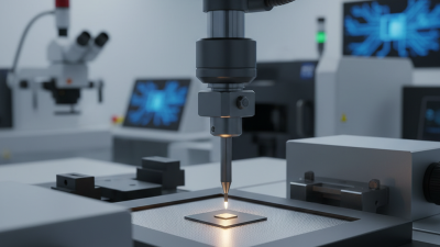
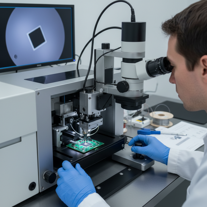
Achieving optimal die placement and alignment is crucial for effective applications. Proper alignment ensures that the die bonds securely, enhancing reliability. One common technique involves using a microscope to check the positioning. This helps in identifying misalignments that are not visible to the naked eye. It’s important to maintain a clean workspace to avoid contamination. Dust and debris can impact the bonding process.
Another technique is utilizing alignment pins. These can help guide the die into the correct position. However, some users find the pins can be cumbersome. If not placed correctly, they may obstruct the alignment process. Regular practice is necessary to master this method. It is essential to adjust and recalibrate frequently, as this can lead to better outcomes.
Temperature control is also vital for die bonding. Variations in temperature can affect adhesive properties and die placement. Experiment with different temperatures to find an optimal condition. However, monitoring this aspect requires constant attention, which can be challenging. It is easy to overlook minor fluctuations that could result in alignment issues later. Adapting and learning from these experiences is part of mastering die bonding techniques.
Common Challenges in Die Bonding and Their Solutions
Die bonding is a critical process in microelectronics. Challenges can arise, impacting the final product’s quality. One common issue is improper alignment. This can lead to poor electrical connections. A misaligned die may create excess stress during the bonding phase. Careful setup and calibration of the bonding tool can mitigate this problem.
Thermal management is another challenge. Excessive heat can damage sensitive components. It is crucial to monitor temperatures during the die bonding process. Using proper heat sinks and thermal interfaces can help disperse heat effectively. Sometimes, operators overlook this aspect, leading to failures.
Contamination can also be problematic. Dust and particles can interfere with the bonding quality. Maintaining a clean workspace is essential. Regular cleaning of tools and surfaces can reduce contamination risks. Each step must be scrutinized, as neglecting one small detail can have severe consequences. The die bonding process requires attention to detail and a willingness to adapt.
How to Use Die Bonding Tool for Effective Applications? - Common Challenges in Die Bonding and Their Solutions
| Challenges |
Details |
Possible Solutions |
| Alignment Issues |
Misalignment during die bonding can lead to failures. |
Use precision alignment tools and fixtures. |
| Thermal Stress |
Thermal differences can cause warping of materials. |
Implement controlled heating and cooling processes. |
| Adhesive Failure |
Improper adhesion can lead to device failure. |
Select appropriate adhesives tested for the application. |
| Contamination |
Dust and oils can affect bonding quality. |
Ensure cleanroom environments and proper handling. |
| Poor Process Control |
Lack of monitoring can lead to inconsistencies. |
Implement automation and monitoring systems. |