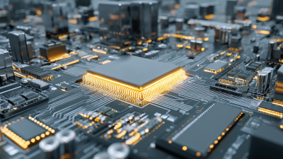
10 Unique Benefits of Die Bonding in Semiconductor Manufacturing
In the ever-evolving landscape of semiconductor manufacturing, die bond technology plays a crucial role in ensuring the reliability and performance of electronic devices. As the demand for smaller, faster, and more efficient components escalates, manufacturers are increasingly leveraging die bonding techniques to enhance their production processes. This guide explores ten unique benefits of die bonding, highlighting its significance in reducing production costs, improving thermal conductivity, and enhancing overall yield. From advanced materials to innovative processes, die bond practices not only streamline manufacturing but also contribute to the longevity and efficiency of semiconductors. Understanding these benefits is essential for industry professionals aiming to stay ahead in a competitive market, making this guide an invaluable resource for optimizing semiconductor production through effective die bonding strategies.
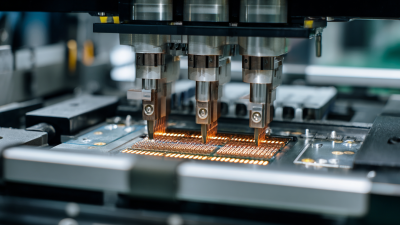
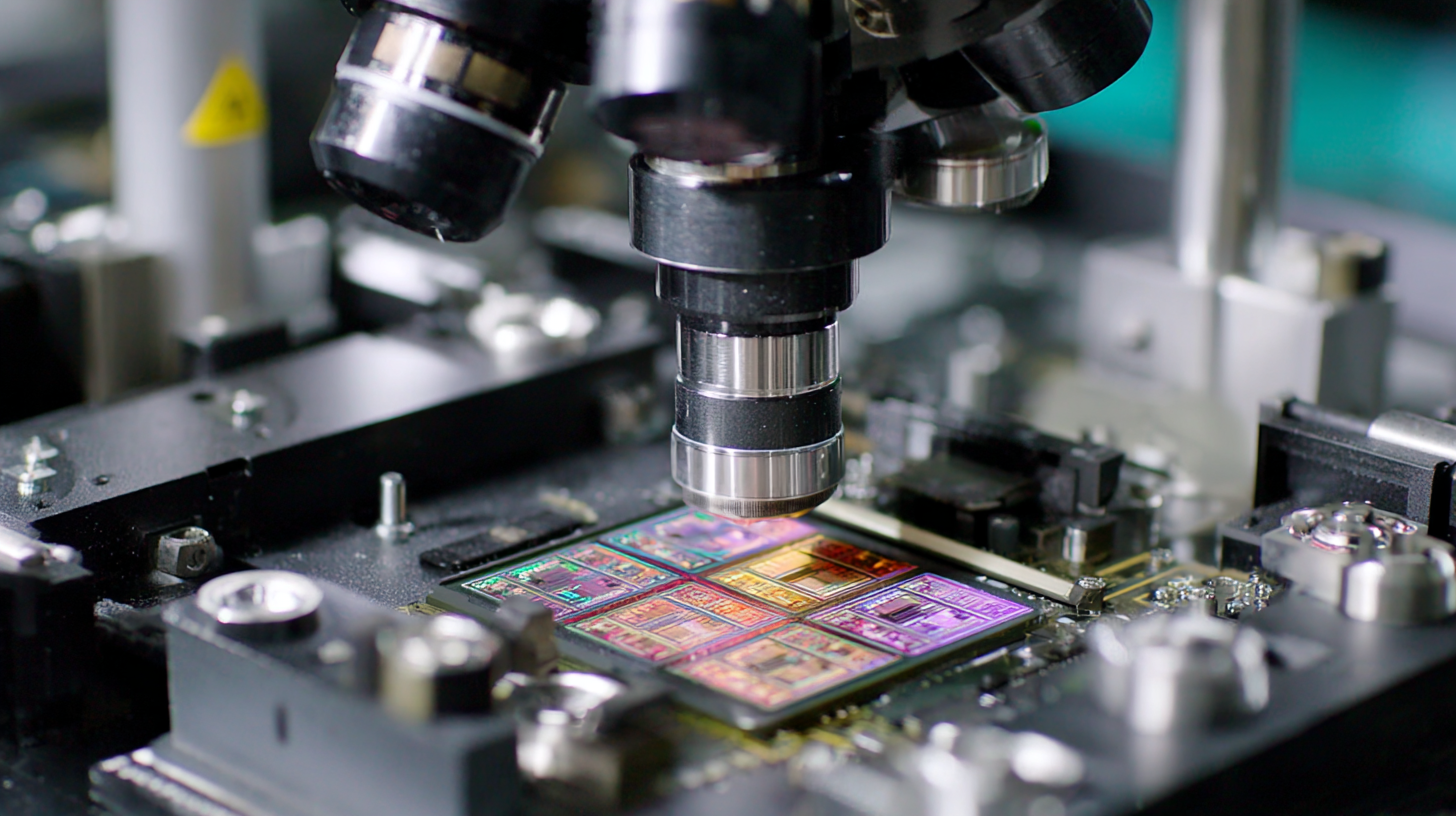
Understanding Die Bonding: An Overview of its Role in Semiconductor Production
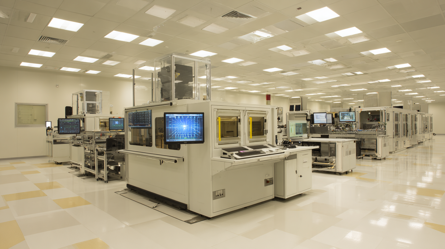
Die bonding is a critical process in semiconductor manufacturing, playing a vital role in ensuring the performance and reliability of integrated circuits. This technique involves attaching a semiconductor die to a substrate, which is essential for enabling electrical connections and thermal management. A recent report by IC Insights highlighted that the global semiconductor market is expected to reach $1 trillion by 2030, underscoring the importance of die bonding in meeting increasing production demands.
The die bonding process typically employs various materials and methods, such as epoxy, solder, or adhesive, which can impact the overall efficiency and lifespan of semiconductor devices. According to a study by Yole Développement, the die bonding equipment market is projected to grow at a CAGR of 6.4% over the next five years. Advances in automated die bonding technologies are enabling manufacturers to achieve greater precision and scalability, which are essential for producing complex, high-performance chips used in areas like AI and automotive applications. As the industry evolves, understanding die bonding's role becomes increasingly crucial for semiconductor professionals aiming to enhance manufacturing capabilities and product quality.
10 Unique Benefits of Die Bonding in Semiconductor Manufacturing
This chart illustrates the unique benefits of die bonding in semiconductor manufacturing, highlighting 10 key advantages.
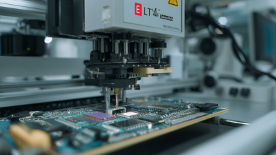
Enhanced Thermal Management through Die Bonding Techniques
Die bonding techniques in semiconductor manufacturing play a crucial role in enhancing thermal management, particularly with the increasing emphasis on high-performance electronics. By vertically stacking multiple semiconductor components, such as chips or dies, manufacturers can significantly improve thermal conductivity and dissipation. This advanced packaging technique not only boosts performance but also reduces power consumption and minimizes the overall footprint of the devices.
One of the unique benefits of using die bonding is its ability to optimize heat flow within the semiconductor modules. Innovative approaches, such as through-silicon vias (TSVs) and thermal interface materials, contribute to more effective heat transfer between dissimilar materials. As industries like electric vehicles, renewable energy, and 5G technology continue to evolve, the demand for enhanced thermal management solutions will only increase. Thus, die bonding is positioned as a key enabler in addressing the thermal challenges associated with modern high-power applications, fostering improved reliability and longevity of semiconductor devices.
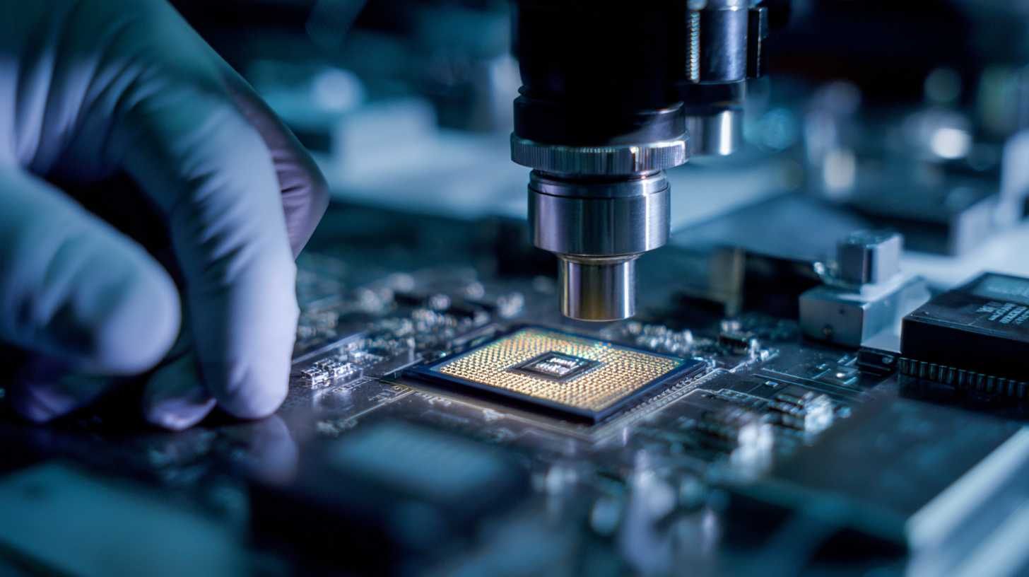
Improving Electrical Performance with Advanced Die Bonding Methods
In the rapidly evolving landscape of semiconductor manufacturing, advanced die bonding techniques are becoming increasingly crucial for enhancing electrical performance. Among these methods, die attach films and silver sintering technologies are leading the charge. Forecasts indicate a significant growth in the die attach film market, projected to expand from USD 1.2 billion in 2024 to USD 2.5 billion by 2033, driven by the demand for improved interconnection methods. These advancements not only promise better thermal management but also contribute to the miniaturization of components, thereby optimizing overall device efficiency.
Moreover, as the semiconductor industry strives to meet the growing demands of electric mobility and renewable energy systems, innovative bonding techniques such as E-Stack bonding emerge as vital solutions. These methods facilitate the integration of lightweight, high-performance materials within electric motors, enhancing their efficiency and sustainability. This trend is further reflected in the notable increase anticipated in the semiconductor bonding market, expected to reach around USD 1,400 million by 2034. Such advancements ensure that manufacturers can deliver sophisticated, high-performing products that cater to the needs of modern technology applications while maintaining robust electrical performance.
Cost Efficiency: How Die Bonding Optimizes Semiconductor Manufacturing
Die bonding plays a critical role in enhancing the cost efficiency of semiconductor manufacturing. This process involves permanently attaching a semiconductor die to a package or substrate, significantly reducing the overall material costs and time involved in production. According to a report by SEMI, the global semiconductor manufacturing market is expected to reach $556 billion by 2025, indicating a robust demand for efficient methods like die bonding that can streamline operations and reduce waste. By optimizing the die bonding process, manufacturers can not only minimize labor costs but also improve yield rates, leading to significant savings.
To further enhance cost efficiency in die bonding, manufacturers can adopt specific tips. First, selecting the right die attach materials can prevent common issues such as thermal and mechanical stress, which could otherwise lead to increased failure rates and higher production costs. Second, regular maintenance of bonding equipment ensures consistent, high-quality outputs, reducing the chances of defects that can inflate operational expenses. Lastly, implementing automation in the die bonding process can save labor costs while enhancing precision, ultimately leading to lower overall production costs.
As the semiconductor industry continues to evolve, leveraging die bonding innovations will be essential for manufacturers to stay competitive. By focusing on these strategies, companies can achieve cost efficiencies that not only benefit their bottom line but also position them for future growth in an increasingly demanding market.
The Future of Die Bonding: Innovations and Trends in the Industry
Die bonding plays a crucial role in semiconductor manufacturing, and its future is poised for significant transformation driven by innovations and industry trends. According to a report from MarketsandMarkets, the die bonding equipment market is projected to reach USD 4.5 billion by 2025, growing at a CAGR of 6.2%. This growth highlights the increasing demand for high-precision bonding processes that improve the reliability and performance of semiconductor devices. As technology evolves, we see the emergence of advanced die bonding techniques, such as thermosonic and laser bonding, which promise enhanced efficiency and reduced manufacturing costs.
Moreover, sustainability is becoming a focal point in die bonding trends, with companies increasingly adopting eco-friendly materials and processes. A study by SEMI indicates that the semiconductor industry is committed to reducing its carbon footprint, and innovative die bonding technologies are at the forefront of these efforts. The integration of AI and machine learning in manufacturing processes is also set to revolutionize quality control in die bonding, ensuring higher precision and fewer defects. As we look to the future, the synergy of these technological advancements and sustainable practices will undoubtedly redefine the landscape of die bonding in semiconductor manufacturing.