5 Compelling Reasons Why Bonding Wire and Ribbon Are Essential for Modern Semiconductor Manufacturing
In the fast-evolving landscape of semiconductor manufacturing, the critical role of Bonding Wire and Ribbon cannot be overstated. As the demand for smaller, more powerful electronic devices continues to surge, it is projected that the global semiconductor market will reach a staggering $1 trillion by 2030, according to a recent analysis by IC Insights. Bonding Wire and Ribbon are pivotal in ensuring reliable connections in integrated circuits, enabling higher performance, reduced size, and enhanced thermal management. Industry studies indicate that approximately 80% of the semiconductor packaging process relies on advanced bonding technologies, underscoring the importance of selecting the right materials. With innovations in wire and ribbon technologies, manufacturers can optimize production efficiency and meet the increasing performance demands of modern electronics, making Bonding Wire and Ribbon essential components in the semiconductor production ecosystem.

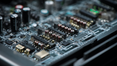
The Critical Role of Bonding Wire in Enhancing Semiconductor Performance
In the fast-paced world of semiconductor manufacturing, the significance of bonding wire cannot be overstated. It serves as a vital link between the semiconductor die and the outside world, ensuring reliable electrical connections that enhance performance. High-quality bonding wire is essential for optimizing signal integrity and thermal management, which directly impacts the efficiency and durability of semiconductor devices. By utilizing advanced materials and techniques, manufacturers can leverage bonding wire to reduce resistance and improve overall device reliability.
The advancements in bonding ribbon technology also play a critical role in modern semiconductor applications. Bonding ribbons, offering superior electrical and thermal conductivity compared to traditional bonding wires, enable manufacturers to create more compact and efficient semiconductor packages. This innovation not only elevates performance metrics but also supports the miniaturization trend in electronics, allowing for the development of smaller, yet more powerful devices. As the demand for high-performance semiconductors continues to grow, the integration of innovative bonding solutions will be pivotal in driving advancements across various applications, from consumer electronics to automotive systems.
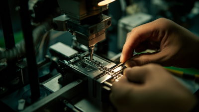
Exploring the Advantages of Ribbon Bonding for High-Density Packaging Solutions
In the rapidly evolving landscape of semiconductor manufacturing, high-density packaging solutions are becoming increasingly critical. Ribbon bonding, in particular, shines as a pivotal method that addresses the growing demands for smaller, more efficient electronic components.
This technique not only enables the connection of multiple die in a single package but also optimizes space by allowing for a flatter configuration. The ultra-fine pitch and wider surface area of ribbon bond leads lead to enhanced electrical performance and heat dissipation, making it ideal for advanced semiconductor applications.

Moreover, the advantages of ribbon bonding extend beyond just space efficiency. With its flexibility in wire routing, ribbon bonding accommodates intricate designs that are characteristic of modern electronics.
This method also offers superior mechanical stability, which is essential in high-stress environments common in today’s technologies. By integrating ribbon bonding into their processes, manufacturers can achieve higher yield rates and reduce potential failures, thus ensuring that high-density packages perform reliably in various applications, from consumer electronics to automotive systems.
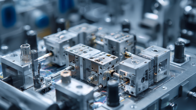
Cost-Effectiveness of Bonding Wires: An Essential Factor in Semiconductor Production
The cost-effectiveness of bonding wires plays a critical role in modern semiconductor production, especially as manufacturers face escalating pressures to enhance efficiency and maintain competitive pricing. As semiconductor devices become smaller and more complex, driven by advancements in artificial intelligence and other cutting-edge applications, the demand for advanced packaging solutions has surged. Bonding wires and ribbons are essential components that not only facilitate the connection between chip and substrate but also help to optimize overall production costs.
Recent trends indicate that the global bonding wire market is expected to reach significant heights, propelled by the increasing requirement for effective semiconductor packaging. This growth is rooted in the industry’s pivot towards more innovative and compact solutions, which rely heavily on efficient wire bonding techniques. By investing in state-of-the-art bonding materials and processes, manufacturers can significantly reduce tool wear, thereby maximizing wire bonding efficiency and minimizing production expenses. This strategic focus on cost-effectiveness will be crucial as the industry navigates the limits of Moore's Law and seeks to enhance chip performance through more advanced back-end production methodologies.
Innovations in Bonding Technologies: Driving Efficiency in Semiconductor Manufacturing
The rapid evolution of semiconductor manufacturing is significantly driven by innovations in bonding technologies, particularly in advanced packaging techniques. The transition from conventional 1D printed circuit board (PCB) designs to sophisticated 3D hybrid bonding at the wafer level is reshaping the landscape. This shift enables ultra-fine interconnections, leading to enhanced performance in high-performance computing (HPC) and a greater capacity to meet the demands of increasingly complex electronic applications.
Furthermore, the rise of 2.5D and 3D packaging materials reflects a broader trend in semiconductor technology towards higher efficiency and optimized power distribution. Manufacturers are increasingly adopting hybrid bonding techniques, which facilitate a more effective interconnect at the chip level, thereby improving thermal management and overall device performance. As the semiconductor industry continues to grow, these innovations in bonding wire and ribbon technologies will be essential for developing the next generation of high-performance chips, ultimately driving efficiency and performance across various electronic platforms.

Impact of Bonding Materials on Thermal Management and Reliability of Semiconductors
The impact of bonding materials on thermal management and the overall reliability of semiconductors is becoming increasingly crucial in modern manufacturing practices. As the semiconductor industry rapidly evolves, the demand for effective thermal interface materials (TIMs) and innovative microfluidics has surged. These advancements facilitate superior heat dissipation, which is essential for maintaining optimal performance in power semiconductors and integrated circuits (ICs). Efficient thermal management directly correlates with device reliability, reducing the risk of overheating and ensuring longevity in complex electronic systems.
Moreover, bonding wires and ribbons play a vital role in this equation by providing strong connections that help manage thermal expansion and contraction. The growing semiconductor bonding market highlights the industry's focus on developing advanced materials capable of withstanding high temperatures while maintaining structural integrity. As trends lean towards intricate packaging and more sophisticated devices, the need for reliable bonding solutions becomes imperative. Ultimately, the integration of cutting-edge bonding technologies is key to advancing the efficiency and reliability of modern electronic devices, making them indispensable in the race for innovation in semiconductor manufacturing.
Impact of Bonding Materials on Thermal Management and Reliability of Semiconductors