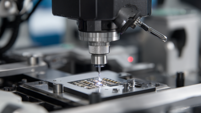
What is Die Bonding Tool and How Does it Work?
The Die Bonding Tool is a crucial component in the semiconductor manufacturing process. It plays a significant role in attaching chips to substrates. This tool ensures strong adhesion and precise placement, which are vital for device performance. Engineers rely on this tool to create reliable connections in various applications.
Understanding the Die Bonding Tool requires insight into its mechanics. It involves a mix of heat and pressure to secure materials effectively. Precision is key, as improper application could lead to failures. Each step in the bonding process requires attention to detail. Even minor errors can impact the final product's quality.
The Die Bonding Tool is not without challenges. Users often face issues like misalignment or inadequate bonding strength. These obstacles necessitate continuous improvement and learning in the field. By examining these aspects, we gain a deeper understanding of the tool's significance. The importance of mastering this technology cannot be overstated in today’s fast-evolving market.
What is Die Bonding Tool?
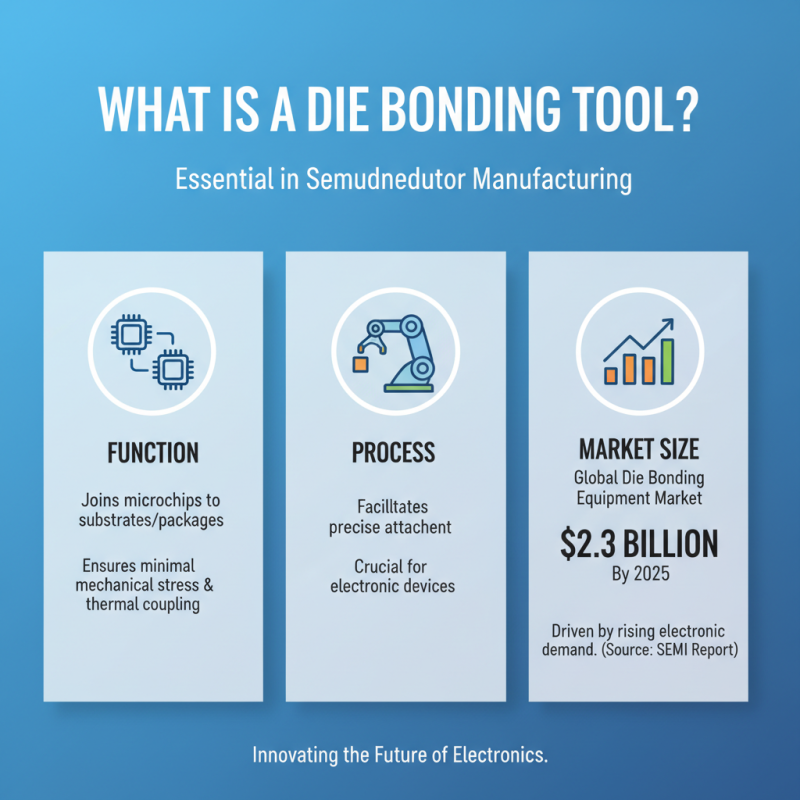
Die bonding tools are essential in various semiconductor manufacturing processes. They facilitate the joining of microchips to substrates or packages, ensuring minimal mechanical stress and thermal coupling. According to a report from the Semiconductor Equipment and Materials International (SEMI), the global die bonding equipment market is projected to reach $2.3 billion by 2025, driven by the rise in electronic device demand.
These tools apply adhesive or solder material precisely to bond the die, ensuring strong connections. An in-depth understanding of material properties, such as thermal expansion and conductivity, is crucial. For instance, a study by the Institute of Electrical and Electronics Engineers (IEEE) highlights the importance of proper adhesive selection, as inappropriate materials can lead to failures in thermal management.
Tips: Always evaluate the thermal and mechanical properties of materials used. This simple step can significantly reduce long-term reliability issues.
Operators must be well-trained to handle die bonding tools effectively. Misalignment during bonding can lead to performance degradation. Regular maintenance of equipment is essential for longevity. Monitoring equipment accuracy helps prevent costly production errors that can arise from tool wear or miscalibration.
Tips: Schedule routine equipment checks. Proactive maintenance can enhance both productivity and efficiency.
The Importance of Die Bonding in Semiconductor Manufacturing
Die bonding is a crucial process in semiconductor manufacturing. It involves attaching a semiconductor die to a substrate using adhesives or solder. This step directly influences the performance and reliability of microelectronic devices. Recent reports indicate that the global die bonding market is projected to grow significantly, reaching an estimated value of $1.7 billion by 2025, driven by increasing demand for compact and efficient electronic devices.
The quality of die bonding directly affects thermal management and electrical performance. Poor bonding can lead to defects like delamination or thermal stress. A study from the Semiconductor Industry Association emphasizes that about 40% of semiconductor failures are linked to bonding issues. Ensuring high bonding strength and low thermal resistance is essential. New techniques, such as using advanced materials or innovative bonding methods, can enhance performance.
Tip: Regularly calibrate your die bonding equipment. Calibration can help maintain accuracy and precision in the bonding process. Additionally, always verify the integrity of your die before bonding. Minor defects can escalate into significant reliability issues down the road. Emphasizing meticulous quality control can mitigate risks in semiconductor manufacturing.
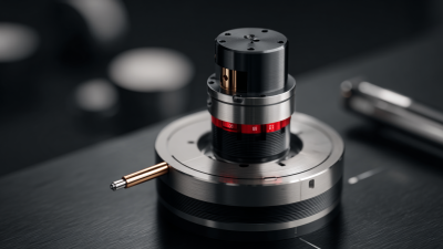
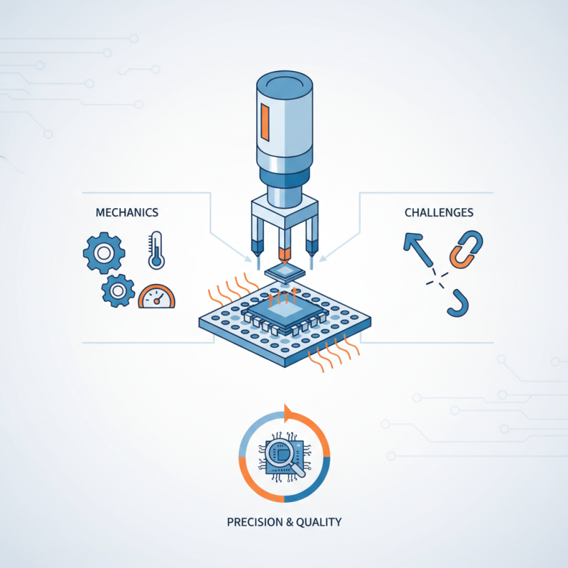
Components and Structure of a Die Bonding Tool
Die bonding tools are essential in semiconductor packaging. Their design includes several key components that ensure effective chip attachment. The main parts are the worktable, heating elements, alignment systems, and robotic arms. Each piece plays a crucial role in precision assembly.
The worktable typically features advanced temperature control. This is critical as temperatures need to be precisely managed. Many industry studies show that improper thermal management can reduce bonding quality by up to 30%. This statistic highlights the worktable's importance in the die bonding process.
Heating elements often use infrared technology. They provide rapid, consistent heating for efficient bonding. The alignment systems, which incorporate optical sensors, ensure accurate placement of the die. Robotic arms facilitate quick, precise movements, improving overall efficiency. However, even with these advancements, human error remains a factor in 5-10% of processes. Continuous improvements in technology aim to minimize these issues and enhance reliability in die bonding operations.
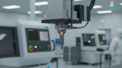
The Die Bonding Process: Step-by-Step Guide
The die bonding process is crucial in semiconductor manufacturing. It involves attaching a semiconductor die onto a substrate or package. This process ensures that electrical connections are made effectively. A precise die bonding tool is essential for this task.
To begin, the die bonding tool picks up the die from a wafer. It uses robotic arms and specialized vacuum technology. Once positioned, the tool applies adhesive or solder to bond the die to the substrate. This step must be accurate; misalignment can lead to device failure.
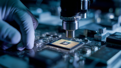
After bonding, the assembly undergoes inspection. Sometimes, defects like air bubbles or misalignment creep in. These issues require careful review. Quality control is critical here. Overall, understanding the die bonding process helps improve yield and product reliability. Making small adjustments can lead to significant enhancements in production efficiency.
Applications and Innovations in Die Bonding Technology
Die bonding technology plays a critical role in the semiconductor industry. This process involves attaching semiconductor chips to their substrates. The accuracy of die bonding directly impacts the performance and longevity of electronic devices. Recent innovations have led to improved techniques, enhancing efficiency and reliability.
One notable application is in automotive electronics. As vehicles become smarter, the demand for efficient die bonding increases. Advanced methods are streamlining this process, reducing production costs while boosting performance. Another area seeing growth is in consumer electronics. With the proliferation of compact devices, precise die bonding solutions are essential for maintaining space and functionality.
However, challenges remain. Some techniques may yield inconsistencies, affecting quality. Engineers are continually refining methods to address these issues. As advancements in materials and processes emerge, the die bonding landscape continues to evolve. Further research is vital to overcome current limitations and enhance overall reliability in this technology.