Best Die Bond Techniques for Effective Bonding Solutions?
Die Bond techniques play a crucial role in semiconductor manufacturing. The effectiveness of these methods can significantly impact performance and reliability. Renowned Die Bond expert, Dr. Emily Chen, once stated, "Choosing the right bonding method is essential for optimal device functionality."
In the industry, various Die Bond techniques exist, each with its pros and cons. Some methods provide excellent thermal conductivity, while others ensure strong adhesion. However, not all methods are suitable for every application. This variability requires careful consideration when selecting a technique.
Problems can arise during the bonding process. Inconsistent results or inadequate adhesion can lead to device failures. It is vital to continuously refine these techniques. Industry professionals must remain adaptable, ready to innovate and improve. Each choice in the Die Bonding process shapes the future of semiconductor technology.
Overview of Die Bonding Techniques in Semiconductor Applications
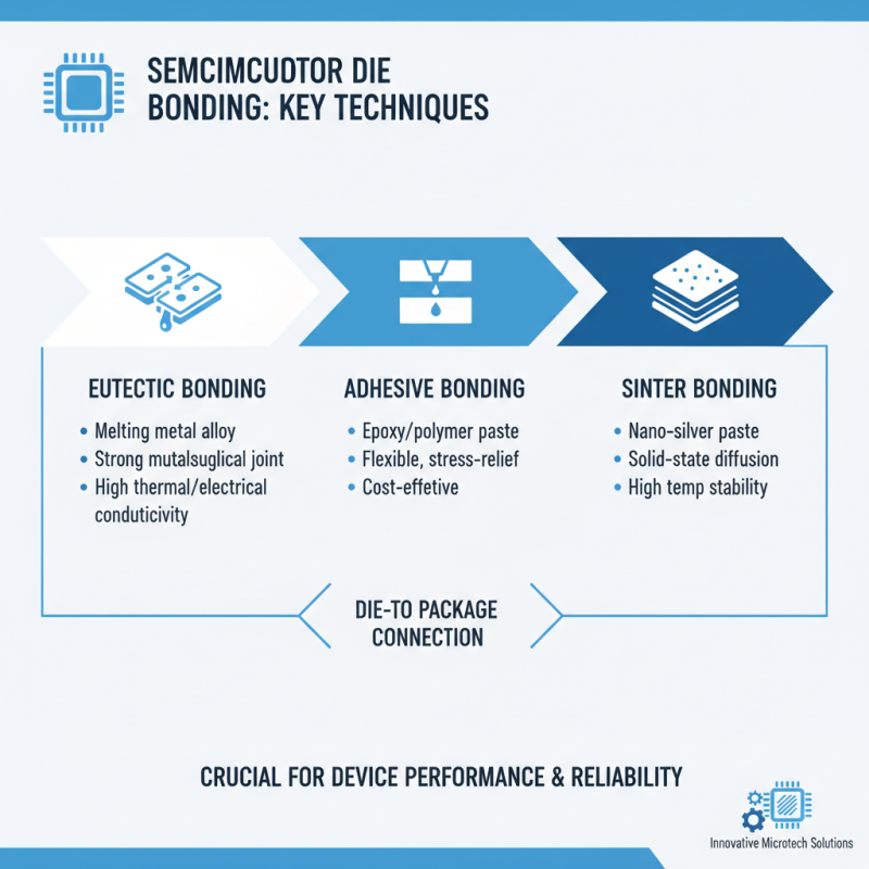
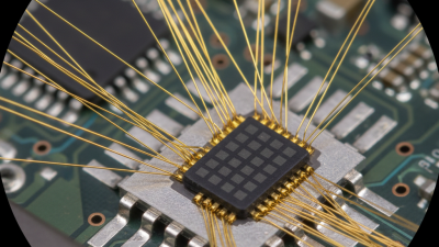
Die bonding is crucial in semiconductor manufacturing. It connects the die to the package. There are several die bonding techniques, each with its unique advantages and challenges. Understanding these methods is vital for effective bonding solutions.
One common technique is epoxy die bonding. This method uses adhesive to attach the die. It provides strong adhesion and is suitable for various applications. However, curing times can be long, leading to production delays. Another method is solder die bonding. This technique involves melting solder between the die and substrate. It offers excellent thermal and electrical performance. Yet, controlling the temperature can be tricky, risking damage to sensitive components.
Flip chip bonding is another technique in the spotlight. This approach flips the die upside down to make direct connections to the substrate. It allows for higher integration density. Unfortunately, this method requires precise alignment and can be costly. Each die bonding method has its own merits and drawbacks. Evaluating these options carefully is essential for optimal performance in semiconductor applications.
Common Materials Used in Die Bonding Processes
Die bonding is essential in semiconductor packaging. The process requires specific materials to create strong and reliable connections. Common die bonding materials include epoxy, silicone, and various metal alloys. Each material possesses unique properties that make it suitable for different applications.
For instance, epoxy adhesives often serve as the primary choice due to their excellent thermal stability. They bond well to silicon, ceramic, and metal surfaces. Some reports indicate that nearly 45% of die bonding uses epoxy. On the other hand, silicone materials provide flexibility and greater tolerance to thermal expansion. They are used when stress management is crucial.
Metallic alloys, such as gold and aluminum, are also prevalent. Gold provides a strong and conductive bond, while aluminum is cost-effective. The usage of these materials can vary widely across industries. In automotive and aerospace, reliability is paramount. A study showed that improper material choice can lead to a failure rate as high as 20% in bonding applications. This emphasizes the need for careful material selection.
Best Die Bond Techniques and Common Materials Used in Die Bonding Processes
Step-by-Step Guide to Die Bonding Methods
Die bonding is crucial in semiconductor manufacturing. Selecting the
right method improves reliability and performance. Different
techniques include epoxy, solder,
and thermocompression bonding. Each has unique characteristics and
is suited for specific applications.
When using epoxy bonding, ensure proper surface preparation. Cleanliness affects
adhesion strength significantly. Studies show that 30% of bonding
failures stem from inadequate surface treatment. A simple solvent wipe could enhance the bond.
Thermocompression bonding is another effective method. It requires precise temperature
control and pressure application. According to industry reports, poorly managed thermal conditions lead to
25% reduced effectiveness. Monitoring parameters is essential for
success.
Tip: Always perform a test bond before the full process.
This practice saves time and material by identifying issues early.
Ultimately, understanding each technique's benefits and limitations leads to better bonding solutions. A reflective
approach may further improve outcomes in future projects.
Evaluating the Performance of Different Die Bonding Techniques
Die bonding is a crucial process in semiconductor manufacturing. It directly affects the reliability and performance of electronic devices. Different die bonding techniques have been developed to enhance these properties. A 2022 report by Yole Développement highlighted that, among various methods, adhesive bonding showed a notable increase in thermal conductivity. This makes it a popular choice.
Evaluating the performance of these techniques reveals important insights. For instance, eutectic bonding is well-known for its strong electrical connectivity. However, it requires high temperatures, which might not be suitable for all materials. A study indicated that while eutectic bonding achieves excellent results, it can lead to thermal stress issues over time.
Moreover, ultrasonic die bonding has emerged as an innovative technique. It offers quick processing times and lower temperatures compared to traditional methods. Yet, it also presents challenges, such as the need for precise control. Inconsistent parameters can lead to poor bond quality and lower yields. Understanding these nuances is essential for optimizing production processes.
Future Trends in Die Bonding Technologies and Innovations
Die bonding technology is evolving rapidly. Innovations in materials and processes change the landscape. Companies are exploring new adhesives and bonding methods that save time and enhance strength. This shift drives the need for better performance at lower costs.
Tips: Stay updated on market trends. Experiment with emerging materials. This can lead to solutions that boost efficiency.
Automation is another key trend. Robots are becoming essential in the die bonding process. They offer precision and reduce human errors. However, the challenge lies in integrating these technologies smoothly. Training staff can be difficult but is essential for success.
Tips: Invest in training programs for your team. Explore collaborative robots to ease the transition. Reflect on your current processes and identify areas for improvement.
Sustainability is gaining attention. Eco-friendly adhesives are on the rise. Companies are urged to consider the environmental impact of their materials. Traditional processes often leave a significant carbon footprint. Adopting greener practices may require time and effort, but it is worth exploring.
Tips: Research sustainable alternatives. Assess the recyclability of your materials. Continuous reflection will help refine methods and reduce waste.